- Pro
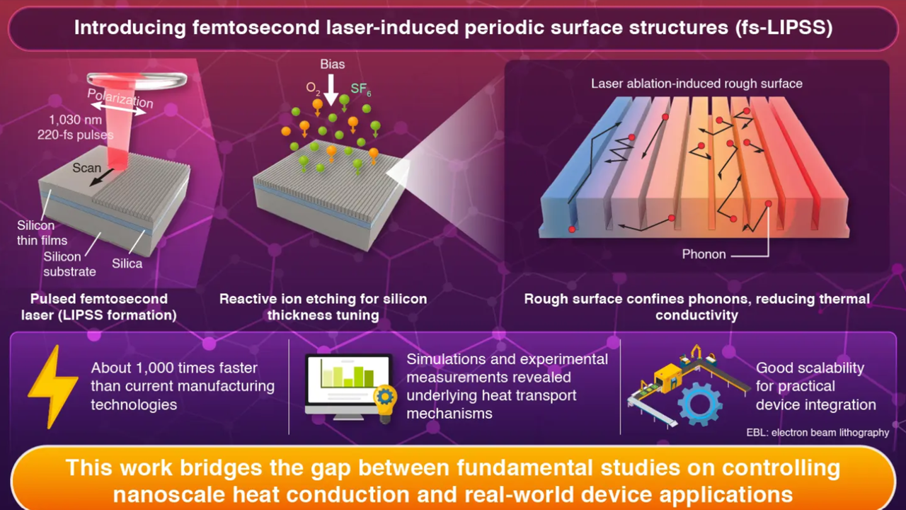
Thermal conductivity drops due to controlled phonon scattering distances
When you purchase through links on our site, we may earn an affiliate commission. Here’s how it works.
 (Image credit: ISCT)
Share
Share by:
(Image credit: ISCT)
Share
Share by:
- Copy link
- X
- Threads
- Heat flow is altered inside chip components instead of removed after buildup
- Phonon motion is limited through nanoscale surface patterning
- Ultrafast lasers enable nanoscale patterning at industrially relevant speeds
Today, most electronics rely on heat sinks, fans, or liquid cooling because the components inside chips conduct heat in fixed ways.
A new method designed by Japanese researchers lets engineers control how fast heat escapes from a material, rather than just trying to remove heat after it builds up.
The work describes a laser-based fabrication method that modifies how heat moves through thin silicon and silica films by directly shaping their surfaces at the nanoscale.
You may like-
 Magnets produced at room temperature using lasers could one day produce better HDDs, faster non-silicon processors — and at 20nm, they are so thin that they could be used almost anywhere, even in the human body
-
 Not exactly a DeepSeek moment for AI accelerators - but this Chinese optical chip may well be 100x faster than Nvidia's A100 on some tasks
-
 HBM-on-GPU set to power the next revolution in AI accelerators - and just to confirm, there's no way this will come to your video card anytime soon
Altering heat transport at the chip component level
The approach relies on ultrafast laser pulses, each lasting a femtosecond, to ablate material and create parallel grooves across the film surface.
These grooves form with carefully controlled spacing and depth that closely match the average distance phonons travel before scattering.
Because phonons are the primary carriers of heat in these components, restricting their movement predictably alters overall thermal conductivity.
The resulting features, known as femtosecond laser-induced periodic surface structures, show high uniformity over relatively large areas.
Are you a pro? Subscribe to our newsletterContact me with news and offers from other Future brandsReceive email from us on behalf of our trusted partners or sponsorsBy submitting your information you agree to the Terms & Conditions and Privacy Policy and are aged 16 or over.When combined with conventional dry etching to adjust film thickness, the patterned surfaces exhibit a marked reduction in thermal conductivity.
Thermoreflectance measurements quantified this change, offering experimental confirmation rather than inferred behavior.
Numerical simulations also showed that the reduction arises mainly from limited phonon travel distances rather than changes in chemical composition or bulk material properties.
You may like-
Magnets produced at room temperature using lasers could one day produce better HDDs, faster non-silicon processors — and at 20nm, they are so thin that they could be used almost anywhere, even in the human body
-
Not exactly a DeepSeek moment for AI accelerators - but this Chinese optical chip may well be 100x faster than Nvidia's A100 on some tasks
-
HBM-on-GPU set to power the next revolution in AI accelerators - and just to confirm, there's no way this will come to your video card anytime soon
A central claim of the study concerns fabrication speed. The fs-LIPSS process is reported to operate at a throughput more than 1000x faster than single-beam electron-beam lithography while still achieving nanoscale resolution.
This difference is substantial, especially for applications requiring large patterned areas, such as thermal layers integrated into data center-class processors.
The process is maskless and resist-free, which reduces procedural complexity and aligns with standard CMOS manufacturing constraints.
The technique has also been described as capable of wafer-scale implementation without introducing additional components or lithographic steps.
Because the method avoids resists and masks, it remains compatible with established semiconductor workflows.
The researchers describe the process as scalable, semiconductor-ready, and suitable for integration with existing fabrication lines.
The nanostructures are described as mechanically robust, with reports indicating strength levels up to 1000x higher than those produced using some conventional patterning approaches.
However, the available description provides limited detail on direct mechanical benchmarking or comparative testing methods.
The technique appears promising, and it is relevant for high-performance computing, quantum devices, and thermal management challenges associated with dense GPU clusters powering modern AI tools.
But wider adoption will depend on reproducibility, long-term stability, and cost under industrial conditions, especially at data center deployment scales.
Via Institute of Science Tokyo
Follow TechRadar on Google News and add us as a preferred source to get our expert news, reviews, and opinion in your feeds. Make sure to click the Follow button!
And of course you can also follow TechRadar on TikTok for news, reviews, unboxings in video form, and get regular updates from us on WhatsApp too.
 Efosa UdinmwenFreelance Journalist
Efosa has been writing about technology for over 7 years, initially driven by curiosity but now fueled by a strong passion for the field. He holds both a Master's and a PhD in sciences, which provided him with a solid foundation in analytical thinking.
Show More CommentsYou must confirm your public display name before commenting
Please logout and then login again, you will then be prompted to enter your display name.
Logout Read more Magnets produced at room temperature using lasers could one day produce better HDDs, faster non-silicon processors — and at 20nm, they are so thin that they could be used almost anywhere, even in the human body
 Not exactly a DeepSeek moment for AI accelerators - but this Chinese optical chip may well be 100x faster than Nvidia's A100 on some tasks
 HBM-on-GPU set to power the next revolution in AI accelerators - and just to confirm, there's no way this will come to your video card anytime soon
 The future of chips: how gate-all-around design is powering the AI era and the next node
 Project Silica rival plans to launch 500GB Proof-of-concept medium in 2026 — but questions remain about speed, durability, and cost
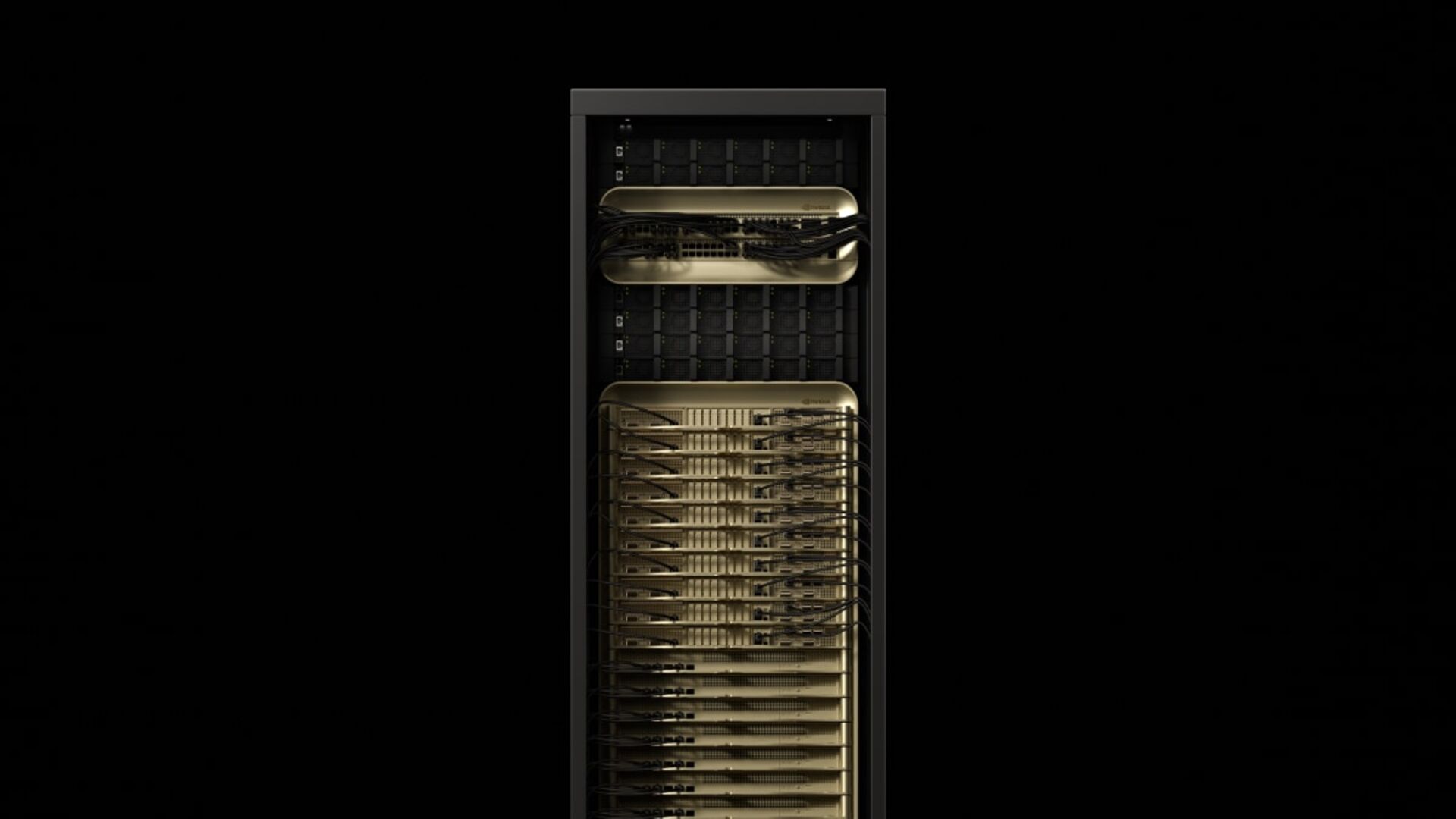 Got a spare $50,000? Cooling a single Nvidia Blackwell Ultra NVL72 rack costs as much as a Tesla Model Y - and it's only going to get more expensive with new racks
Latest in Pro
Got a spare $50,000? Cooling a single Nvidia Blackwell Ultra NVL72 rack costs as much as a Tesla Model Y - and it's only going to get more expensive with new racks
Latest in Pro
 Best n8n hosting
 Forget lasers and missiles, China wants to kill drones using a common tech households use everyday in kitchens all around the world — invisible microwave weapons can fry electronics but still require line-of-sight and proximity
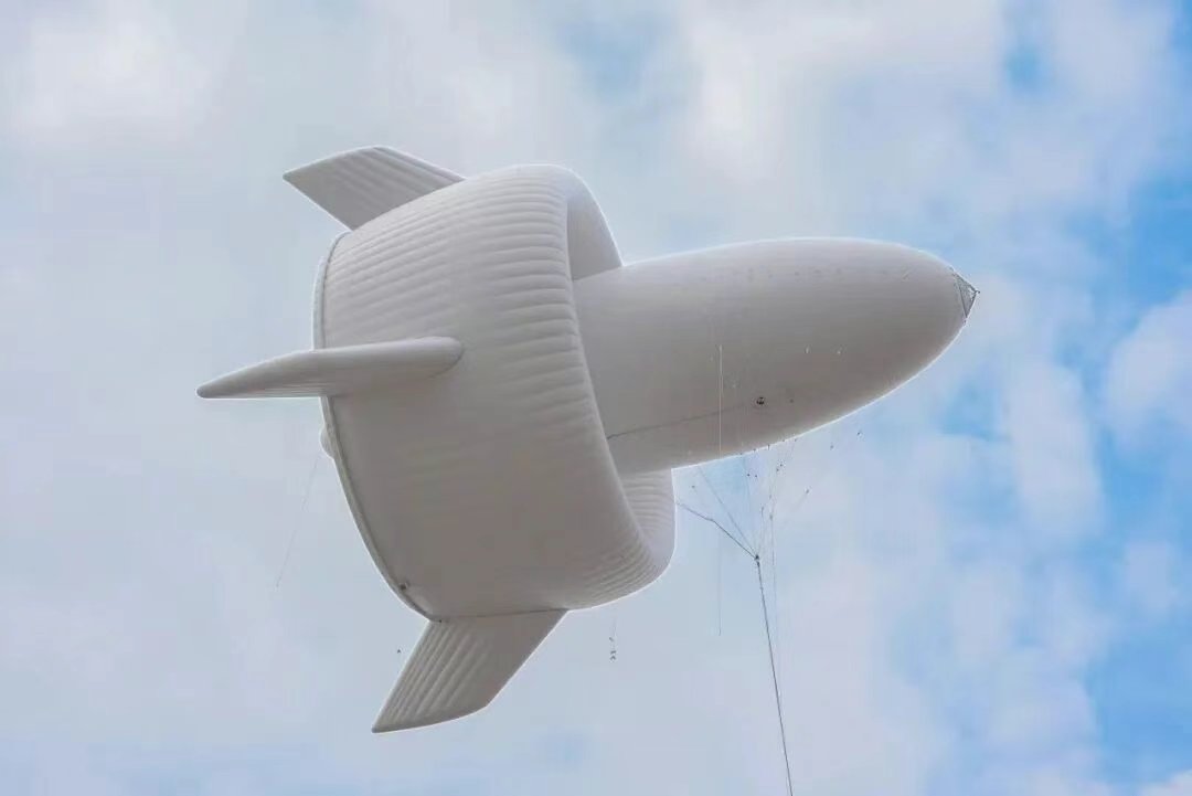 'It’s like wrapping the wind from all sides': Drone-like airship with 24 blades is world's first megawatt-class tethered wind turbine — S2000 rises to 2Km and can generate a whopping 3MW
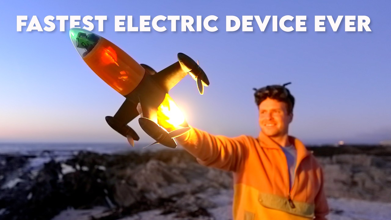 A 3D printed drone is probably the world's fastest DIY plane ever, quicker than even the legendary P38 Lightning — but at 408mph, it has some way to go to catch up with the 575mph TU-95
 7 high-converting print-on-demand products to add to your website
 5 income streams you can add to your website right now
Latest in News
5 income streams you can add to your website right now
Latest in News
 Apple's OLED touchscreen MacBook Pro upgrade could arrive early
 Samsung Galaxy S26 leak shows no sign of the Pro or Edge models
 ChatGPT ads are coming — OpenAI confirms and explains how they'll work
 ‘People love the unexpected’ — Disney on the Lego Star Wars Smart Play launch
 ICYMI: the week's 7 biggest tech stories like Apple losing to Google, and Meta giving up on VR
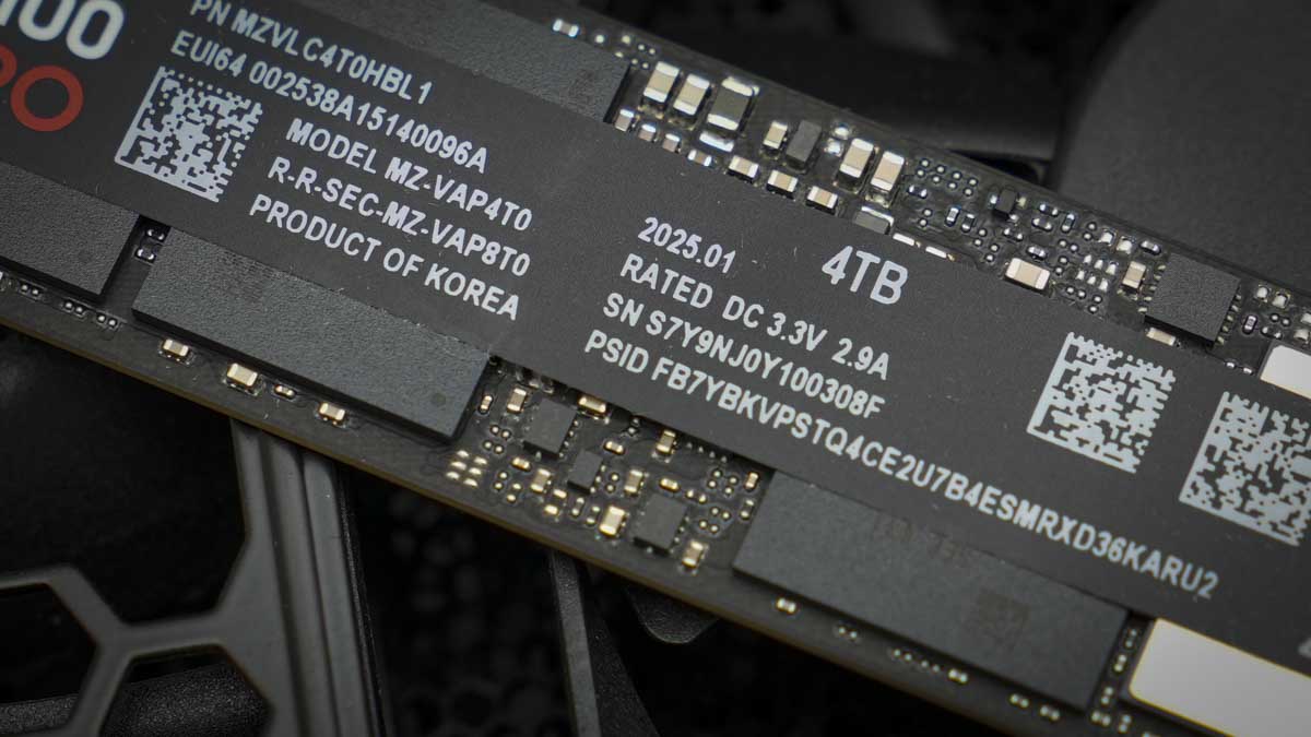 Some top-end SSDs are now literally worth more than their weight in gold
LATEST ARTICLES
Some top-end SSDs are now literally worth more than their weight in gold
LATEST ARTICLES- 1A laser that can fire light pulses in one billionth of a second is set to produce structures 1000 times stronger, 1000 times faster — novel technique has applications for high-performance computing, quantum devices, and AI chip cooling
- 2DRAM prices set to almost double by March 2026, and yes, we all have our AI overlords to thank for that wonderful news
- 3This Sony camera is smashing it and I'm not surprised – it’s ranked no.1 in multiple best-selling lists and now our top camera buying guides
- 4Apple's OLED touchscreen MacBook Pro upgrade could arrive early
- 5'It’s like wrapping the wind from all sides': Drone-like airship with 24 blades is world's first megawatt-class tethered wind turbine — S2000 rises to 2Km and can generate a whopping 3MW